 |
 |



Hobby Electronics |

Do It Yourself |
|||||||
|
|||||||
|
|||||||
 This space is dedicated to the publication of low-cost and easy-to-implement projects, with an emphasis on bench instrumentation. These are for honest, intelligent people who respect copyright laws and show respect for others, refraining from causing noise pollution. This space is dedicated to the publication of low-cost and easy-to-implement projects, with an emphasis on bench instrumentation. These are for honest, intelligent people who respect copyright laws and show respect for others, refraining from causing noise pollution. |
|||||||
|
|||||||
 |
|||||||
by FM Timi |
|||||||
| Building one’s own instruments is a common activity in the hobby of electronics. And, a gain or hFE meter is always useful on the experimenter’s or professional’s workbench. |
|||||||
| The present instrument was designed to measure the current gain of low and medium power bipolar junction transistors (BJT), commonly found in TO-92, TO-18, TO-126, and other packages. |
|||||||
| The circuit is simple and easy to assemble and use. It assists in the pairing (matching) of transistors in hFE or in choosing the most suitable unit for a specific project. |
|||||||
| Preamplifiers and high-fidelity amplifiers, discrete digital-to-analog converters, instrumentation, and regulated power supplies are examples of applications where transistors matched in hFE are almost always required. Whether in differential stages, transconductance amplifiers, current mirrors, or other circuits. |
|||||||
| We know that conventional transistors (not Darlington) rarely have gains greater than 800. Therefore, an instrument that measures up to 2000 is already suitable. The circuit presented here goes a bit further, providing gain readings of up to approximately 6800. |
|||||||
| In the present meter, the hFE is directly proportional to the measured voltage and corresponds to 1 mV per unit of gain. That is, for a gain equal to 10, we will have 10 mV; for gain 100, we will have 100 mV, and so on. |
|||||||
| To simplify assembly and reduce costs, readings are made directly on an external digital voltmeter, connected to the +DVM and -DVM terminals. Or, if the reader prefers, they can assemble a voltmeter based on the ICL7107 or 7106, for example, and incorporate it into the hFE meter. The input resistance of the voltmeter should preferably be greater than 10 MΩ. |
|||||||
| The simplest option, however, would be to use the digital multimeter that the reader already has, setting it to the function of measuring direct current voltage (DCV). |
|||||||
| Most digital multimeters have an input resistance of approximately 10 MΩ across all ranges. And, some models may exhibit a resistance of 100 MΩ or higher in the first continuous voltage scales. All are suitable for the present purpose. |
|||||||
| However, there are questionable digital “multimeters” that may present resistances lower than 10 MΩ, although their manufacturers hide this information or provide untruthful data. |
|||||||
| For example, a popular “multimeter” from a Chinese manufacturer, marketed under different brands, besides having a false safety rating, CAT — endangering the physical integrity of the operator —, presents an input resistance of only 5 MΩ at low voltages, even though the value of 10 MΩ is reported in the technical sheet. |
|||||||
| High-quality multimeters from renowned brands, such as Fluke, Gossen Metrawatt, Hioki, Keysight, Sanwa, and Yokogawa, among others, do not present these problems. They are trustworthy instruments, although they may have a higher cost. Moreover, these are the instruments recommended for use in the bench or field, regardless of whether the reader is a hobbyist or professional. |
|||||||
| Some information about digital multimeters can be found in the fourth part of a series of texts published between 2020 and 2022. This information is available for consultation at the following address: |
|||||||
|
|||||||
| Due to the variables involved in the real world, accuracy is not a priority in an unpretentious hFE meter, like the one presented here. However, it is important that it is precise, allowing us to select transistors with close gains and within the desired range. |
|||||||
| If the reader is interested, more information about accuracy and precision can be found in the same article mentioned earlier. |
|||||||
| Theory |
|||||||
| The collector current (Ic) of a transistor is, in summary, the base current (Ib) multiplied by its hFE. If the base current is known, the hFE can be calculated by measuring the collector current and dividing the obtained value by Ib. Figure 1. |
|||||||
| The emitter current (Ie) will be the sum of the base (Ib) and collector (Ic) currents. |
|||||||
|
|||||||
Figure 1. |
|||||||
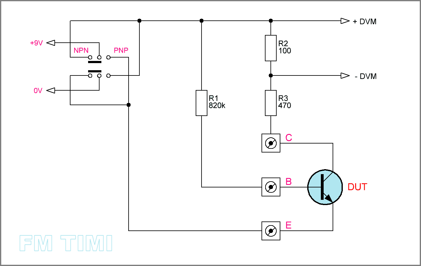
| The simplest example of an hFE meter is probably the one shown in Figure 2. Its excessive simplicity, however, results in limitations. As we can observe, the base current (Ib) is provided by a fixed value resistor (R1), connected to a constant voltage source. Therefore, Ib depends not only on the resistance value of R1 and the supply voltage, but also directly on VBE and the junction temperature. It should be noted that, in transistors, VBE decreases as the temperature increases, resulting, in this case, in an increase in Ib. This aspect alters the value of the hFE measured by this and other meters with this characteristic, making it difficult to match the transistors. |
|||||||
|
|||||||
Figure 2. |
|||||||
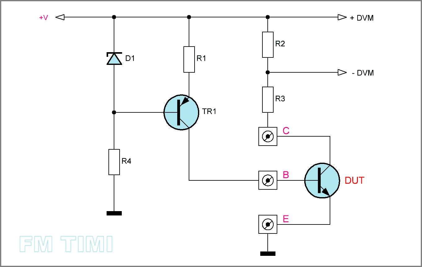
| An improvement of this circuit can be seen in the simplified scheme of Figure 3. In it, the performance was improved with the addition of a constant current source for the transistor base. By stabilizing the base current, it no longer depends on VBE and its respective relationship with the junction temperature. However, for the meter to function properly, there must be two current sources. These sources must be symmetrical and complementary, for the measurement of NPN and PNP transistors, respectively. Obtaining these two symmetrical and complementary currents is not a trivial task. This requires the use of precision circuits, temperature compensated. Compensation is relevant to ensure that the meter’s performance is not affected by variations in ambient temperature. Therefore, a complete instrument will not be as simple as the topology illustrated in Figure 3. In fact, the meter will have a larger number of components and usually two or more current adjustments for the device to be calibrated. When well designed, this circuit can be insensitive to variations in supply voltage. |
|||||||
|
|||||||
Figure 3. |
|||||||
| Circuit Operation Principle |
|||||||
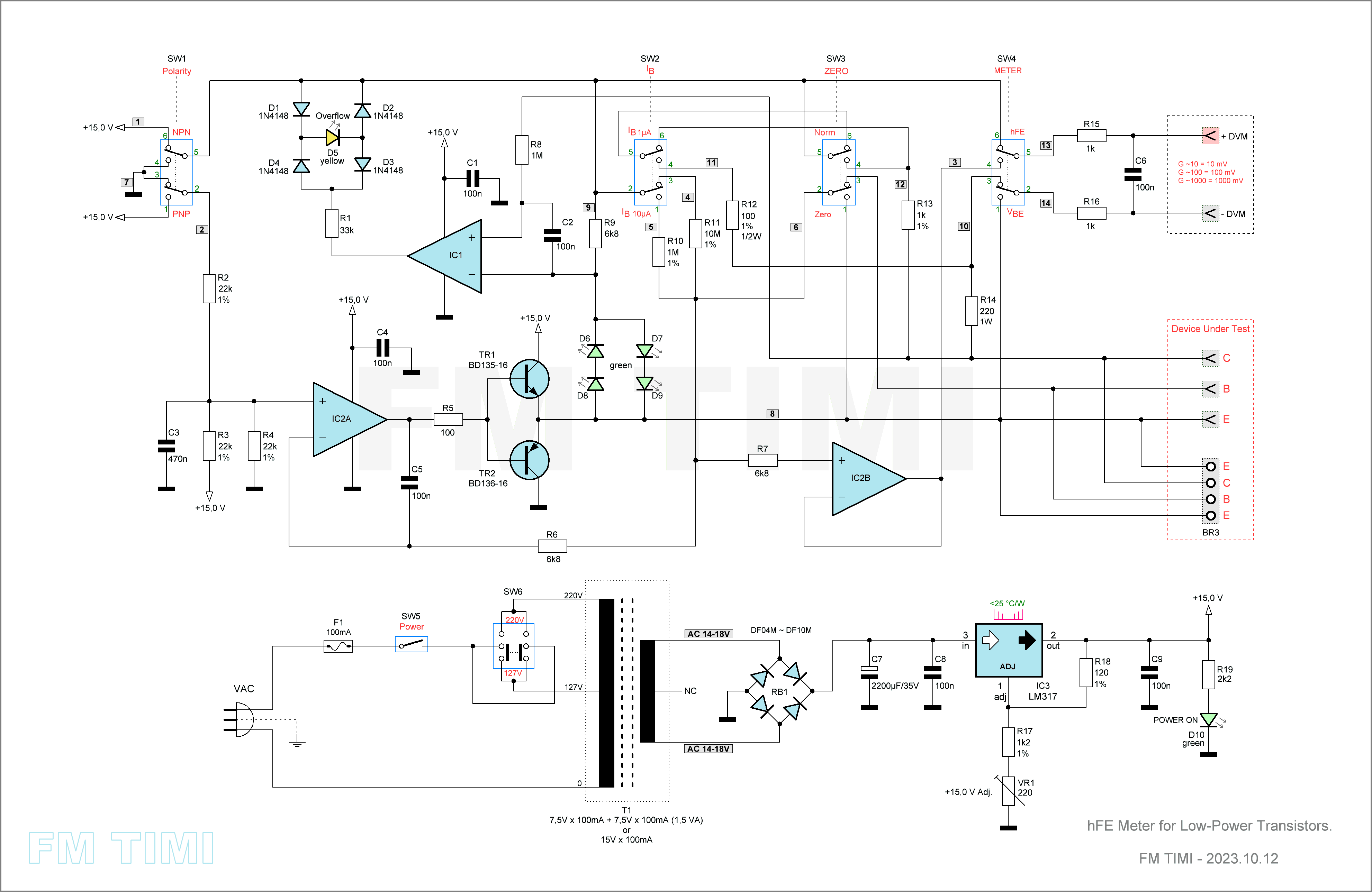
| Figure 4 presents the complete schematic diagram of the hFE meter. |
|||||||
|
|||||||
Figure 4. Click on the diagram to enlarge it. - Clique sobre o esquema para ampliá-lo. |
|||||||
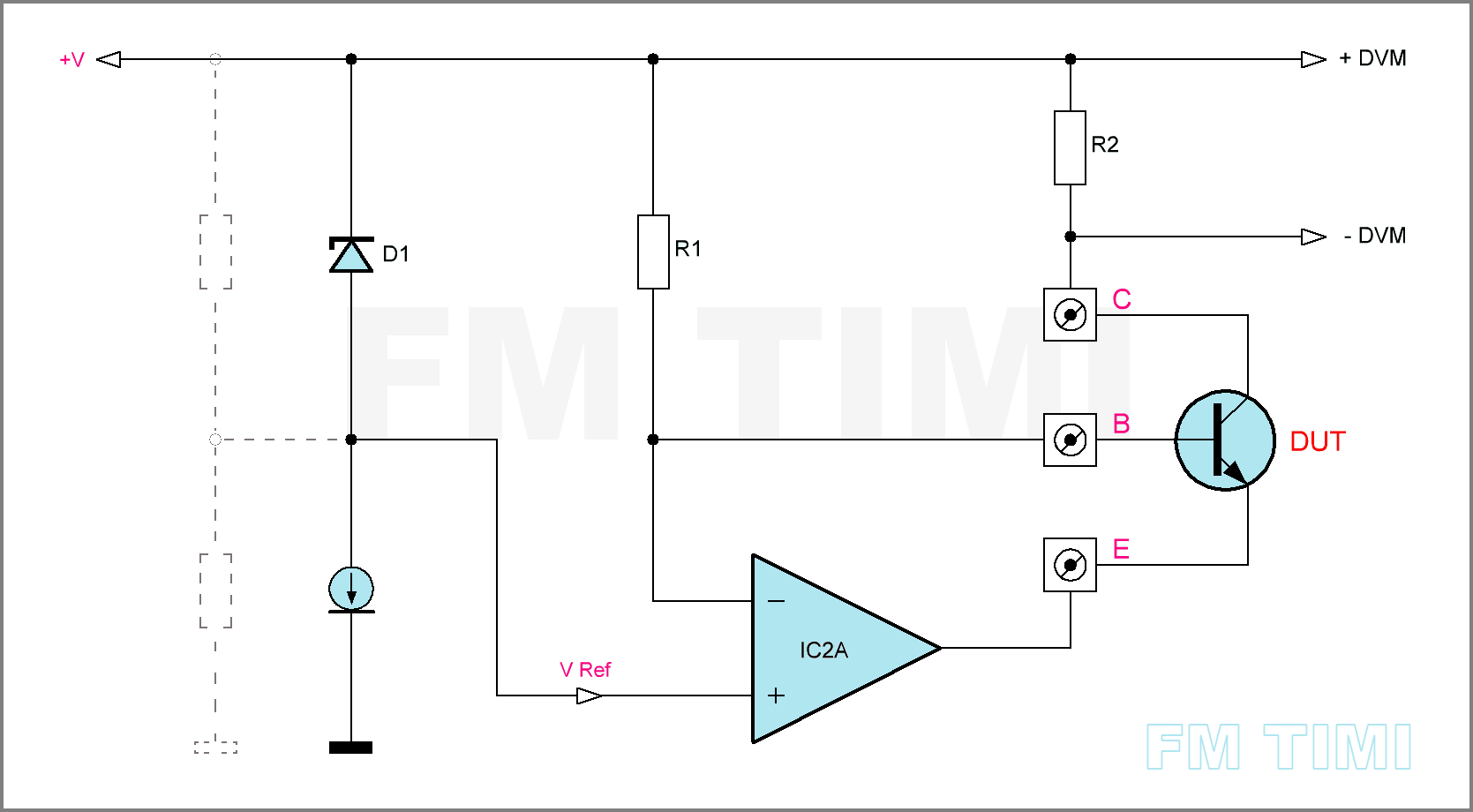
| The basic topology of the circuit is seen in Figure 5 and resembles that of Figure 2, where the base current is supplied by R1. However, now the base-emitter junction of the transistor under test (DUT) is part of the negative feedback loop of an operational amplifier. This amplifier will adjust the emitter voltage to match the potential of the inverting input, as well as the base, to the reference present at its non-inverting input. Thus fixing the voltage at the transistor’s base. Consequently, the current through R1 will remain constant. Given that the base-emitter junction is in series with this circuit, we can conclude that the base current will not be affected by the voltage drop at the junction nor by temperature variations.An additional quality of this stage is to provide equivalent currents for NPN and PNP transistors, with few modifications. |
|||||||
|
|||||||
Figure 5. |
|||||||
| D1 is not a simple Zener diode, as shown in the drawing, but rather a precision reference. This reference can be constituted by an integrated circuit and some external components, or exclusively by discrete components, depending on the available options and the desired technical characteristics. This will ensure that the base current remains independent of fluctuations in the supply voltage.Due to the requirement for a precise, temperature-stabilized reference, in practice, the circuit will be more complex than illustrated or will require components difficult to acquire in the Brazilian market.For this reason, and with the aim of keeping the project accessible to all, a solution based on a resistive voltage divider was chosen. The choice was made possible because the regulated power supply provides the necessary voltage stability to keep the base current within the parameters required for the project. Therefore, it is essential that the source is correctly adjusted and that the LM317 regulator is of high quality. |
|||||||
| The final circuit is simple, low cost, presenting good thermal stability and current symmetry. |
|||||||
| Despite the performance of the circuit depending, in part, on the operational amplifier used, it is expected that the current asymmetry between NPN and PNP type transistors will be less than 1%. |
|||||||
| The accuracy of the meter proved to be adequate for the purpose of the project, even considering the tolerance of the resistors and other variables. |
|||||||
| The SW1 switch is responsible for determining the appropriate polarity for NPN or PNP transistors. |
|||||||
| IC2A and associated components keep the base current (Ib) of the transistor under test constant. As already explained, this occurs regardless of the junction temperature and the base-emitter voltage (VBE). Contributing to slightly more stable readings, especially when compared to those provided by meters whose Ib directly depends on VBE and temperature. |
|||||||
| The base current of the transistor under test will be 1 µA or 10 µA, depending on the selection made through the SW2 switch. |
|||||||
| For safety reasons, a limit was established for the maximum collector current, or IC (considering the collector and emitter terminals in short circuit). The limit is 10 mA for a base current of 1 µA, and will be 33 mA when the base current is set to 10 µA. |
|||||||
| When there is no electric current passing through the base of a transistor, there should be no significant collector current. This means that the transistor is in cut-off and will not present gain. A defective transistor that presents excessive current leakage can cause incorrect hFE readings and compromise the measurement. |
|||||||
| To verify that, in the absence of base current, the gain reading will be equal to zero, the SW3 switch was added. |
|||||||
| Momentarily, we put this switch in the “Zero” position and check if the voltage displayed on the multimeter is less than 1 mV. Ideally, it should be zero, especially for silicon transistors. After this verification, we can change the position of the switch to “Norm” and perform the hFE reading. |
|||||||
| In the case of a defective transistor or connected with inverted terminals, the D5 LED may light up. |
|||||||
| If the reader notices a leakage current greater than expected for an original transistor, which should be in perfect condition, this may indicate the presence of moisture or contamination by some other agent between the terminals. Washing the transistor with isopropyl alcohol, ideally anhydrous, and drying it well, may be helpful. |
|||||||
|
|||||||
| Germanium transistors present a higher leakage current and should not be confused with defective devices. |
|||||||
| The SW4 switch allows for the alternation between the hFE operation mode and the measurement of the voltage between base and emitter (VBE). Certain applications require transistors matched in both characteristics. |
|||||||
| To pair transistors in VBE, it is crucial that all units under test are at the same temperature. |
|||||||
| The 'overflow' indicator, D5, will light up when the "scale limit" is reached. This occurs when the collector-emitter voltage approaches 3.7 V. This value is approximately the minimum acceptable voltage limit for the use of a transistor in linear audio applications, in high fidelity |
|||||||
| In practice, most hFE measurements will be made with higher voltages, far from this limit. For transistors with gain between 10 and 800, the collector-emitter voltage will be in the range of 8.0 V to 10.5 V. |
|||||||
| This range is considerably more realistic when compared to the voltages available in most semiconductor testers that use microcontrollers. Generally, in these devices, the maximum voltage under the transistor is less than five or even three volts. | |||||||
| For a base current (Ib) value of 1 µA, the 'overflow' indication will occur when the count reaches approximately 6800 (scale with 1 mV resolution). For Ib of 10 µA, the count will be about 2150. These values correspond to the collector currents of 6.8 mA and 21.5 mA, respectively. |
|||||||
| It is important to note that this scale limit indication is not critical and can vary more or less, depending on the characteristics of the LEDs used in positions D6 to D9. It is worth mentioning that these LEDs do not function as indicators. Invariably, two LEDs will be softly lit and two will remain off, depending on the position of SW1. |
|||||||
| The choice of base current, whether 1 µA or 10 µA, will depend on the specific application of the transistor. It is important to consider the estimated current range in the circuit where the transistor under test will be employed. This consideration is fundamental for any hFE measurement, regardless of the type of meter used. |
|||||||
| The D10 LED, when lit, will inform that the device is on and, like D5, it can be installed on the instrument panel. |
|||||||
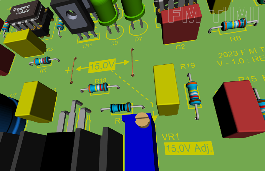
| The power supply, which is quite traditional, should be adjusted to 15 V through the Trimpot® VR1. Two 'jumpers' were added to the printed circuit board to assist in this measurement. Figure 6. |
|||||||
|
|||||||
Figure 6. |
|||||||
| Practice |
|||||||
| The circuit can be housed in a plastic or metal case. The latter is preferable as it serves as shielding. In this case, it should be connected to terminal 3 or 4 of SW1 (circuit GND). It is also advisable to connect it to the "ground" of the electrical installation, when available. |
|||||||
| The power transformer can be 15 V x 100 mA or 7.5 V + 7.5 V x 200 mA. For the latter, the central terminal of the secondary is ignored. |
|||||||
| It is perfectly acceptable to use a transformer with a higher current. |
|||||||
| The discrepancy in the mentioned current is attributed to the practice, common among many manufacturers, of adding the currents of the secondaries of transformers with central derivation or three wires. |
|||||||
| Therefore, a transformer marketed as 7.5 V + 7.5 V x 200 mA can, in many cases, provide only 100 mA per secondary. |
|||||||
| It is important to pay attention to the voltage/current or VA (volt-ampere) ratio, as it can clarify the "power" of the transformer. This ratio is obtained by multiplying the voltage by the current of each secondary and should always be informed by the manufacturer. If, for example, we find a specification of 1.5 VA for a transformer advertised as 7.5 V + 7.5 V x 200 mA (instead of the expected 3 VA), this means that it offers 100 mA per secondary. |
|||||||
| One of the reasons why manufacturers adopt this practice is the assumption that the consumer will build a simple source with full wave rectification using two diodes (one for each secondary), which will result in the sum of the currents. |
|||||||
| A 9 V + 9 V transformer can be used as an alternative. The heat sink of IC3 was sized considering this option. In normal use, IC3 will operate almost without heating. |
|||||||
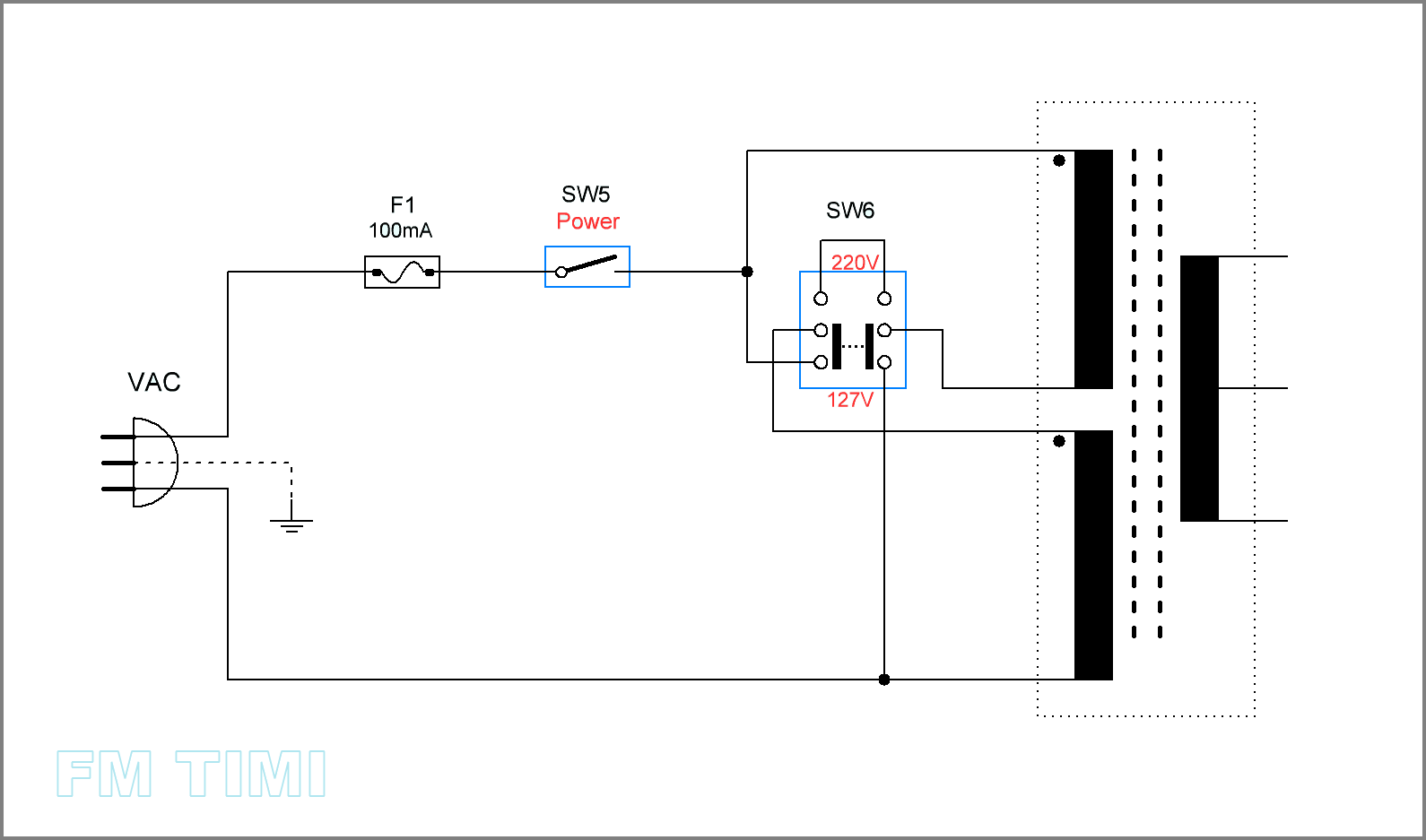
| Most of the small transformers available on the market have three wires in the primary winding, and the electrical diagram was drawn taking this into account. For transformers that have four wires in the primary winding (i.e., two independent primary windings), the reader can be guided by the illustration in Figure 7. |
|||||||
|
|||||||
Figure 7. Click on the diagram to enlarge it. - Clique sobre o esquema para ampliá-lo. |
|||||||
| When the SW6 switch is in the 220 V position, the ideal input voltage will always be double that specified for each primary. However, it is likely that the device will be connected to the main voltage of 127 or 220 V. Therefore, these are the values mentioned in Figure 7. |
|||||||
| For correct operation, it is important to keep both the transformer and the AC input wiring at a safe distance from the rest of the circuit. This distance should be, if possible, greater than 10 cm. |
|||||||
| For the only electrolytic capacitor, of the circuit, I used a Nichicon unit, purchased at the time from Farnell in Brazil. This is because it has been difficult for some time to find good quality electrolytic capacitors in the Brazilian market. Most are of Chinese origin, unknown or counterfeit and, present such low quality that compromises the operation of any electronic circuit. In addition, there is a real danger in using them. As an example, I have already found capacitors whose polarity indication, marked on the encapsulation, was inverted! And an accident did not occur only because I observed that the marking, printed from the negative pole pointed to the longest terminal, when it should correspond to the shortest. A simple test with the multimeter confirmed the error, and upon observing more closely, I found that it was a counterfeit of a Japanese capacitor, from the renowned Rubycon brand. |
|||||||
| A similar problem has already been identified in LEDs of unknown origin, in which the cathode indicator chamfer was wrongly positioned on the opposite side. |
|||||||
| If there is difficulty in acquiring the R12 resistor of 100 Ω by ½ W, this can be replaced by two resistors of 200 Ω by ¼ W, connected in parallel. There is a space provided on the PCB for a second resistor (R12A). |
|||||||
| VR1 is a multi-turn “trimpot”, model 3296W. It is essential that it is from a reliable brand, such as Bourns, Sfernice (Vishay), Spectrol (Vishay), among others, to ensure the stability of the power supply voltage. If it is not possible to acquire the trimpot, it can be replaced by a fixed resistor of 120 ohms, 1%, ¼ W, metal film. With this substitution, we may not exactly obtain 15 V in the power supply, which can result in an accuracy error in the hFE measurement. However, the measurements will still maintain precision. |
|||||||
|
|||||||
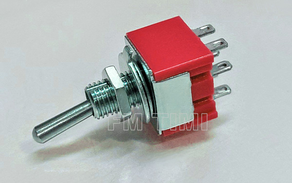
| Once again, attention must be paid to the quality of the components. Many switches found in commerce are of low quality, melting at the time of soldering and/or presenting poor contact. Not coincidentally, they are from Chinese brands or of unknown origin. Some sellers try to hide this by simply saying that the product is "imported". |
|||||||
|
|||||||
| D5 is a high-brightness yellow LED, with a diameter of 3 or 5 mm. Certainly, the reader can opt for LEDs of other colors or types. The only requirement is that it be high brightness. |
|||||||
| On the other hand, D6 to D9 should be common green LEDs of 5 mm with a forward voltage close to 2.1 V, since high-brightness LEDs, which may have a higher forward voltage, are not suitable for these positions. There are LEDs of other colors with a forward voltage of 2.1 V, but the green LED is the most common. |
|||||||
| These LEDs (D6 to D9) are soldered directly on the PCB, but distanced from it by 5 mm or more. | |||||||
| It is important to note that 3 mm LEDs are not recommended for these positions. | |||||||
| I now remember that, in 2009, I recommended to a European manufacturer of High-End equipment to solder the LEDs distanced from the PCB. Unfortunately, this manufacturer seems to have ignored my recommendation. Their practice of soldering the LEDs flush to the board resulted in several defective amplifiers scattered around the world. |
|||||||
| The D10 LED, 3 or 5 mm and green in color, signals that the device is on. The reader is free to choose the model and color they prefer. This is a common LED, not high brightness. |
|||||||
| Although there are integrated circuits (ICs) more suitable for the IC1 and IC2 positions, low-cost models easily accessible in the Brazilian market were chosen, aiming to facilitate assembly for everyone. |
|||||||
| One of the challenges of electronics is to do what we can with, perhaps, the little we have. |
|||||||
| The ICs can be soldered directly on the PCB, however, the use of sockets with turned pins is convenient. |
|||||||
| Adjustment |
|||||||
| After the assembly is completed and reviewed, it is necessary to adjust the power supply voltage. For this, the device must remain on for approximately thirty minutes. Then, we will adjust VR1 until we obtain exactly 15.0 V between the ‘jumpers’ existing on the PCB. |
|||||||
| Use |
|||||||
| 1 - With the multimeter set to the DCV function, connect the red probe tip to the +DVM terminal and the black probe tip to the -DVM terminal. Then, select the appropriate scale. For example, on a 3 ½ digit or 2000 count multimeter, the 2 V (2000 mV) scale can be used, as it offers the ideal resolution of 1 mV and allows readings up to 2000. |
|||||||
| As we know, small variations of hFE can be rounded. Therefore, for scales with better than 1 mV resolution, a reading of 245.7 mV can be rounded to an hFE of 246. |
|||||||
| 2 - Before connecting the transistor to the meter, it is necessary to select the SW1 switch to the position that corresponds to the polarity of the transistor under test, be it NPN or PNP. |
|||||||
| 3 - Low power transistors, such as TO-92 and TO-18 can have their terminals fitted into a socket, observing the correct arrangement of collector, base and emitter. |
|||||||
| There are specific sockets for transistors. However, these can be difficult to find in Brazil. For this reason, a possible alternative would be to use a female pin bar with a 2.54 mm spacing. Another option to be considered is the segmentation of a socket for integrated circuits, which has turned pins. If you opt for a more durable component, the use of a ZIF (Zero Insertion Force) type socket is a viable option. Feel free to exercise your creativity. |
|||||||
| On the other hand, medium power transistors can be connected with the help of cables with alligator clips or tweezers. These cables should not exceed a length of 20 cm. To not compromise accuracy, during reading it is essential to avoid touching the cable connected to the base with your hands. |
|||||||
| Using terminals and banana pins, for example, 2 mm will facilitate the use of different types of cables. | |||||||
| It is timely to remember that some medium power transistors can have collector maximum currents as low as 50 mA. Even for such, this meter can be used safely, considering that the current is limited to 33 mA and, the dissipation will always be less than 85 mW. |
|||||||
| The connection of the collector with the base should not be reversed, because if this accidentally occurs the current that will flow through the base-emitter junction will be close to 12 mA, when SW2 is in the 1 µA position. And, 37 mA with SW2 in the 10 µA position. Generally, this will not damage the transistor, but there are devices whose maximum base current is very small, which can cause significant changes in its structure. |
|||||||
| 4 - Select the SW2 switch for the appropriate base current. |
|||||||
| 5 - Put the SW4 switch in the 'hFE' position to measure the gain. |
|||||||
| 6 - Momentarily, put the SW3 switch in the 'Zero' position. |
|||||||
| In the multimeter of the example, the expected reading will be '± .000' or '± .001', each count corresponding to a unit of gain. The variation of one count is a natural characteristic of digital instruments. |
|||||||
| When returning the SW3 switch to the 'Norm' position, the hFE value will be displayed on the multimeter display. |
|||||||
| 7 - It will be possible to measure the base-emitter voltage for the selected current, by switching the SW4 switch to the VBE position. |
|||||||
| In the case of PNP transistors, all measured values will be negative. |
|||||||
|
Let's consider the following example: |
||||||
| 1 - Measurement of the gain of the 2N2222: |
|||||||
| To measure the gain of a 2N2222 transistor, select the SW1 switch for the NPN configuration and the SW2 switch for 1 or 10 µA. |
|||||||
| 2 - Measurement of hFE: |
|||||||
| Put the SW4 switch in the hFE position. |
|||||||
| 3 - Initial check: |
|||||||
| Position the SW3 switch at 'Zero' to confirm if the reading on the multimeter is zero or ± 1. |
|||||||
| 4 - Reading of hFE: |
|||||||
| Return the SW3 switch to the 'Norm' position. The value displayed on the multimeter will be the hFE of the transistor. |
|||||||
| 5 - Base-emitter voltage (VBE): |
|||||||
| To obtain the value of the base-emitter voltage, select the SW4 switch for VBE. |
|||||||
|
|
||||||
| PCB |
|||||||
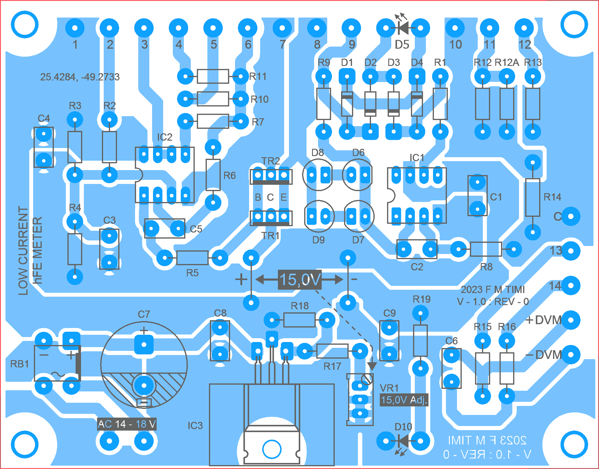
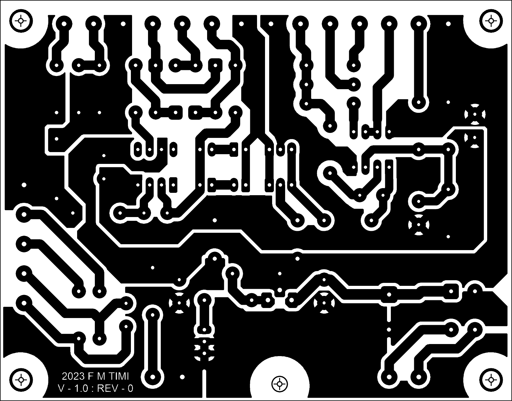
| In Figure 8, a suggestion for the printed circuit board (PCB) is presented. |
|||||||
| The board has dimensions of 110 mm in length by 86 mm in width. |
|||||||
|
|||||||
Figure 8. Click on the image to enlarge it. - Clique sobre a imagem para ampliá-la.
|
|||||||
Copper side of the board illustrated in Figure 8. - (110 mm x 86 mm)
|
|||||||
Click on the image to enlarge it. - Clique sobre a imagem para ampliá-la. |
|||||||
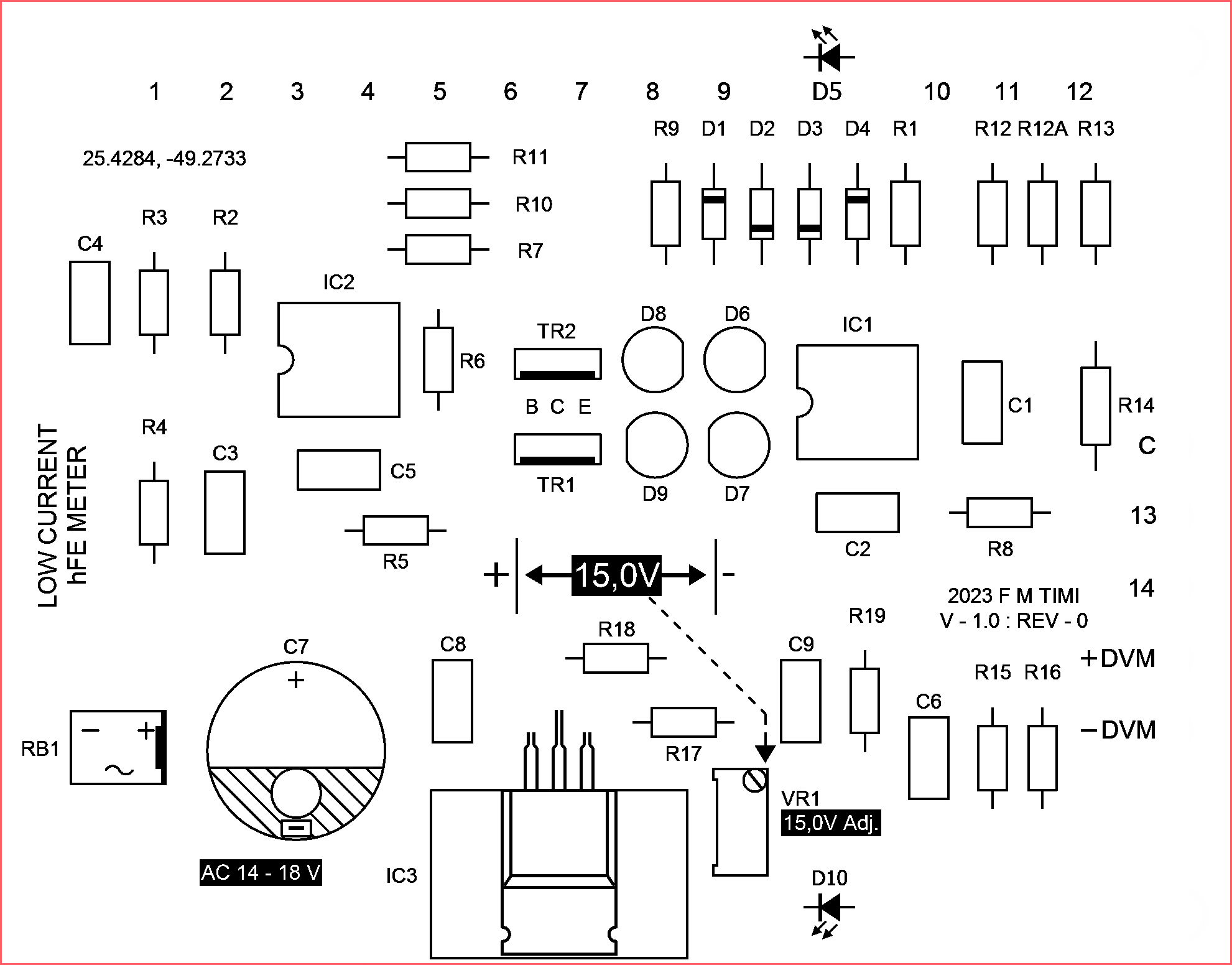
| If the reader chooses to make the printed circuit board through a direct photographic process or screen printing, it may be useful to print the legend of the components, which always facilitates assembly. Figure 9. |
|||||||
|
|||||||
Figure 9. Click on the image to enlarge it. - Clique sobre a imagem para ampliá-la. |
|||||||
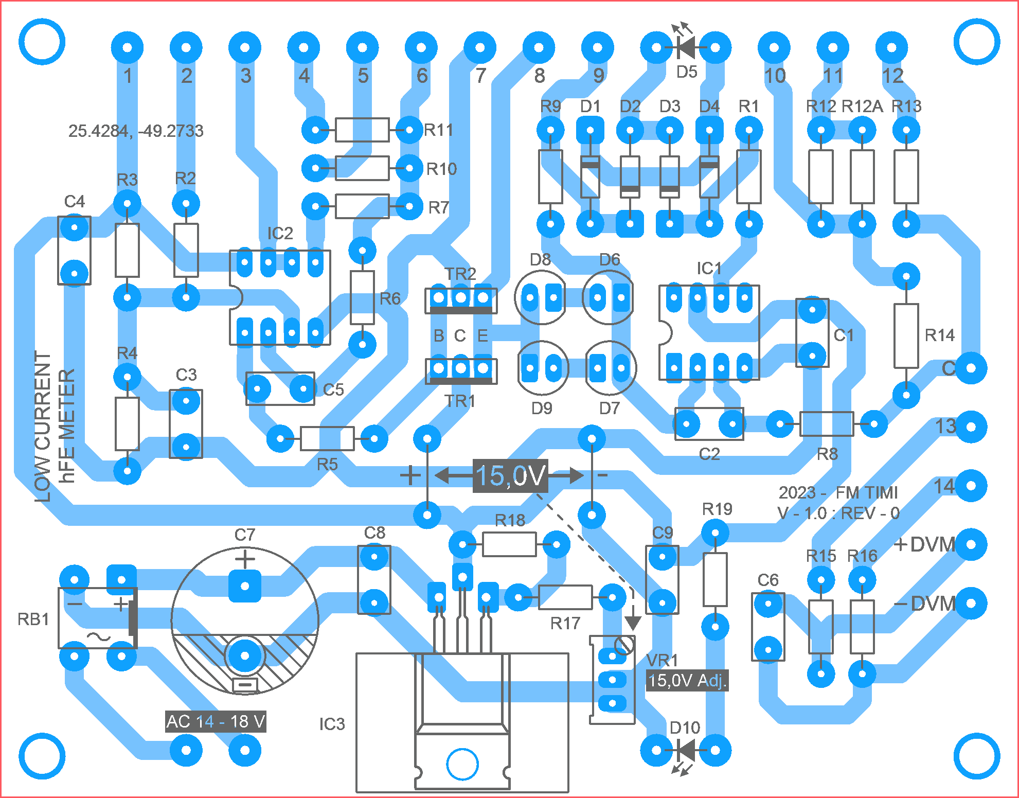
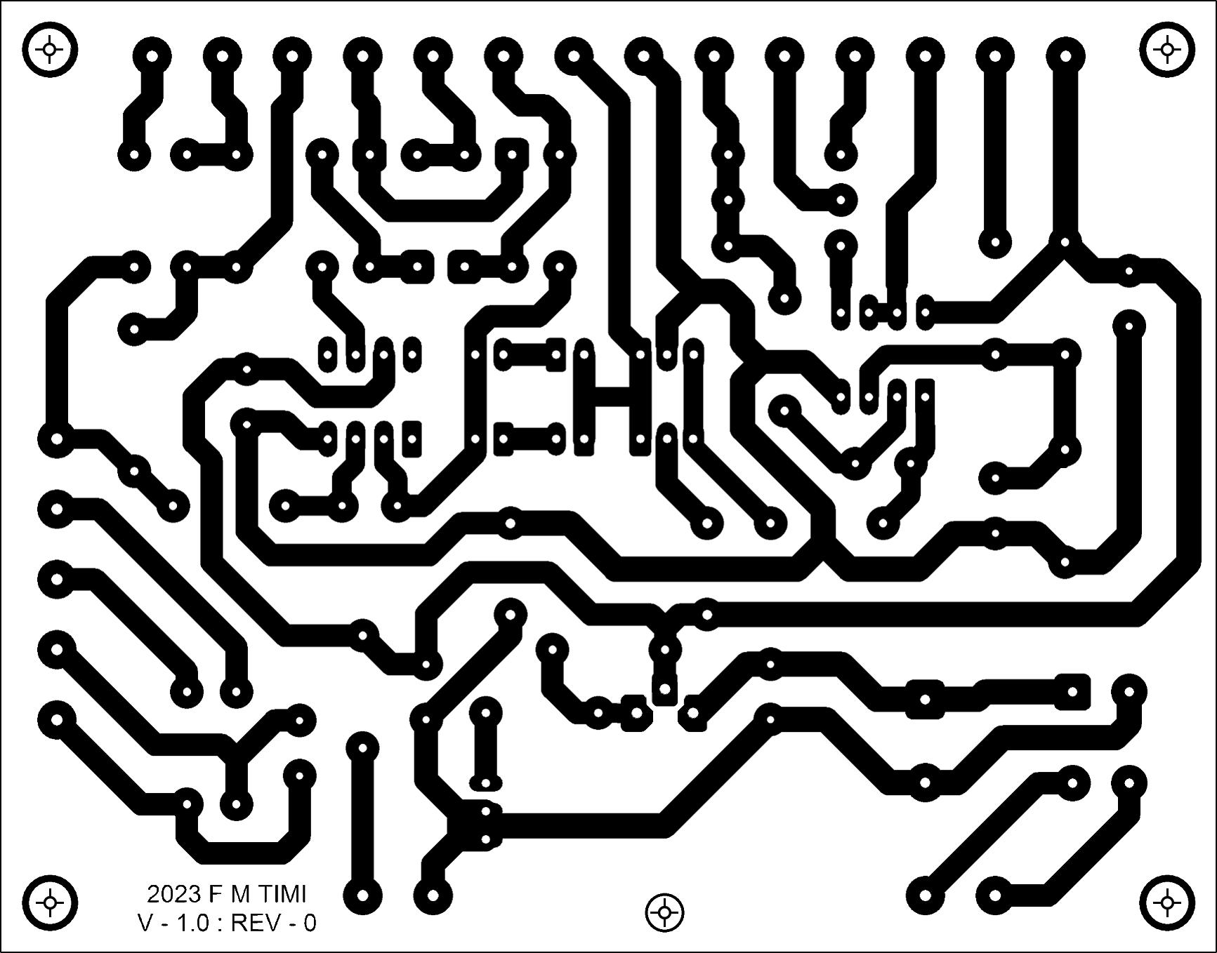
| A simplified version of the board can be appreciated in Figure 10. This version is intended for those who prefer to draw their boards manually. Whether it is a more accessible method or because it is a practice that goes beyond technique and can enter the realm of art. |
|||||||
|
|||||||
Figure 10. Click on the image to enlarge it. - Clique sobre a imagem para ampliá-la. |
|||||||
Cooper side of the board illustrated in Figure 10. - (110 mm x 86 mm) |
|||||||
Click on the image to enlarge it. - Clique sobre a imagem para ampliá-la. |
|||||||
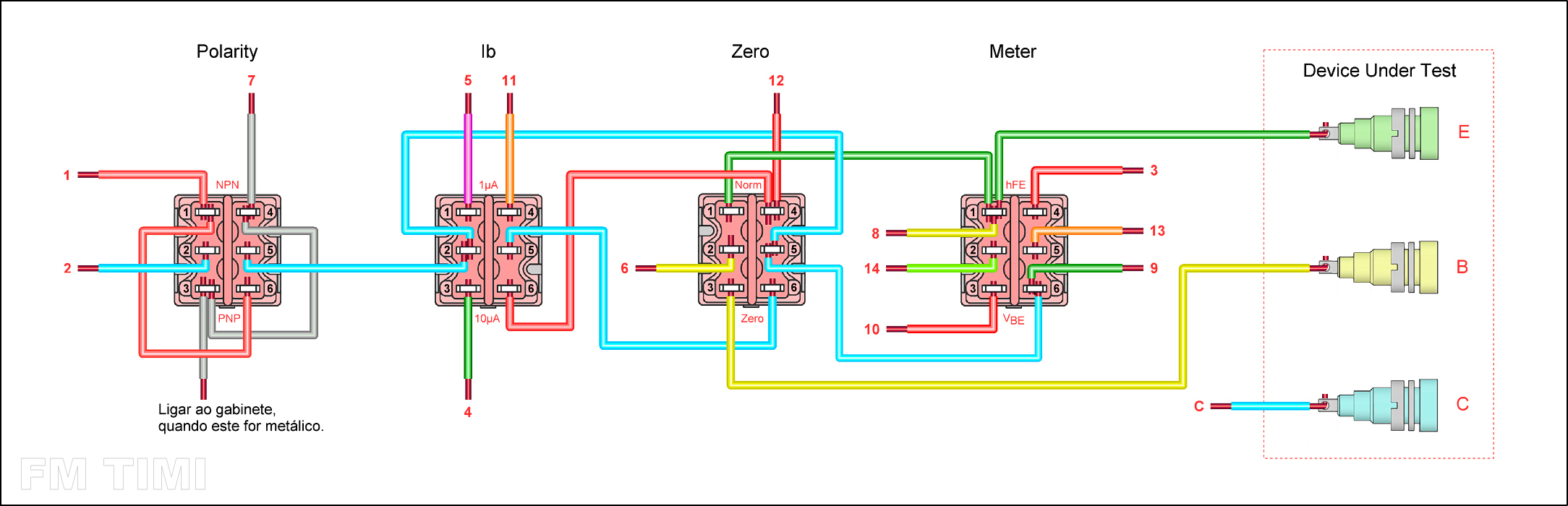
| For the connections of the switches, the reader can guide themselves by the diagram presented in Figure 11. The wire identified as ‘C’, along with those numbered from 1 to 14, should be connected to the corresponding points on the printed circuit board. |
|||||||
|
|||||||
Figure 11. Click on the image to enlarge it. - Clique sobre a imagem para ampliá-la. |
|||||||
| Due to the nature of the project, which deals with high resistance values, it is essential that the printed circuit board be made of fiberglass (FR4). As for the assembly, no special care is needed beyond the usual. It is recommended to properly clean the PCB and the components, avoiding direct contact of the hands with the faces of the board. In addition, it is always good practice to test the components before assembly, thus ensuring the efficiency and safety of the project. |
|||||||
| Component List (PCB) |
|||||||
| Semiconductors |
|||||||
| IC1 – Operational amplifier integrated circuit, DIP8: TL071 or TL081. |
|||||||
| IC2 – Dual operational amplifier integrated circuit, DIP8: TL072 or TL082. |
|||||||
| IC3 – Voltage regulator integrated circuit, TO-220: LM317 or LM217. |
|||||||
| D1, D2, D3, D4 – Diode 1N4148, 1N4150, 1N4151, 1N4448, 1N914, 1N916 or BAW62. |
|||||||
| D5 – High brightness LED, yellow or red (3 mm or 5 mm) - See text. |
|||||||
| D6, D7, D8, D9 – 5 mm diameter green LEDs (T-1 ¾), forward voltage 2.1 V – See text. |
|||||||
| D10 – Green LED (3 mm or 5 mm) – See text. |
|||||||
| RB1 – Bridge Rectifier DF04M, DF06M, DF08M, DF10M or equivalent. |
|||||||
| TR1 – Transistor BD135-16, BD137-16, BD139-16, BD135-10, BD137-10 or BD139-10. |
|||||||
| TR2 – Transistor BD136-16, BD138-16, BD140-16, BD136-10, BD138-10 or BD140-10. |
|||||||
| Resistors |
|||||||
| R1 – 33 kΩ, 1% or 5%, ¼ W, metal film or carbon film. |
|||||||
| R2, R3, R4 – 22 kΩ , 1%, ¼ W, metal film. |
|||||||
| R5 – 100 Ω, 1%, ¼ W, metal film. |
|||||||
| R6, R7, R9 – 6k8, 1%, ¼ W, metal film. |
|||||||
| R8, R10 – 1 MΩ , 1%, ¼ W, metal film.. |
|||||||
| R11 – 10 MΩ , 1%, ¼ W, metal film. |
|||||||
| R12 – 100 Ω, 1%, ½ W (0,5 W), metal film – See text. |
|||||||
| R13, R15, R16 – 1 kΩ , 1%, ¼ W, metal film. |
|||||||
| R14 – 220 Ω, 5%, 1 W, metal film or carbon film. |
|||||||
| R17 – 1k2, 1%, ¼ W, metal film. |
|||||||
| R18 – 120 Ω, 1%, ¼ W, metal film. |
|||||||
| R19 – 2k2, 1% or 5%, ¼ W, metal film or carbon film. |
|||||||
| Adjustable resistor |
|||||||
| VR1 – 220 Ω or 200 Ω, ‘Trimpot’ type 3296W or similar. See text. |
|||||||
| Capacitors |
|||||||
| C1, C2, C4, C5, C6, C8, C9 – 100 nF, 63 V or higher, metallized polyester film, 5 mm lead spacing. |
|||||||
| C3 – 470 nF, 63 V, metallized polyester film, 5 mm lead spacing. |
|||||||
| C7 – 2200 µF, 35 V or more, electrolytic, diameter between 16 and 18 mm, lead spacing of 7.5 mm,ripple current greater than 1 A, 2000 hours or more, 85 °C or more.Recommended brands:: BC Components (Vishay), Chemi-Con, Cornell Dubilier, Elna,EPCOS (TDK), Nichicon, Panasonic, Rubycon. - See text. |
|||||||
| Others |
|||||||
| Heat sink for TO-220, 15 mm, VT801 or similar. |
|||||||
| Two units of socket for integrated circuit, 8 turned pins. Optional item. |
|||||||
| My goal is to bring to readers circuits that not only value true electronics, but are also simple and functional. Circuits that can be assembled by both enthusiasts and professionals, using common components available in the scarce Brazilian market for electronic components. This contrasts with my professional work, which sometimes involves complex circuits, which may employ components unavailable in the Brazilian market. |
|||||||
| The symbology I used in this article does not faithfully follow international standards, however, it is widely used in the technical literature of electronics. |
|||||||
| I believe that this hFE meter will be useful for those who have electronics as a hobby or profession. |
|||||||
| Until next time. |
|||||||
|
|
||||||
|
|||||||
| This article was originally written in Portuguese and subsequently translated into English.Distortions or inaccuracies may occur due to the translation.In case of doubts, I recommend consulting the original text in Brazilian Portuguese. |
|||||||
| Um simples medidor de hFE para transistores de baixa potência. |
|||||||
|
Fábio Maurício Timi - 2023.10.12 - 0 |
|||||||


| © Copyright 1997-2025 TIMI AUDIO. All rights reserved | FRAUD ALERT |
 |
|
|
The content of this site is protected by copyright and may not be duplicated, published, rewritten, or redistributed without prior written authorization. |